In the world of building products and construction, an established divide governs how two types of materials come into being. Biobased materials, such as wood or cotton, are grown; whereas abiotic materials like steel or concrete are not grown, but processed from raw materials.
Recent scientific advances are undermining this distinction. New emerging technologies reveal that abiotic materials may also be grown, and that they—like their biological counterparts—can benefit from some of the characteristics of natural growth compared to traditional industrial manufacturing.
This transition from additive, subtractive, or assembly-based fabrication models to approaches that resemble biological development opens up new possibilities, including resource efficacy, construction efficiency, and multifunctionality. As with biological materials, abiotic substances that are grown—rather than assembled piece by piece—can result in products with less waste, fewer interfaces, and increased functional capacities. The following examples illustrate the shifting boundary between fabrication and formation. Although these are nascent discoveries, they represent significant long-term implications for architecture and design.
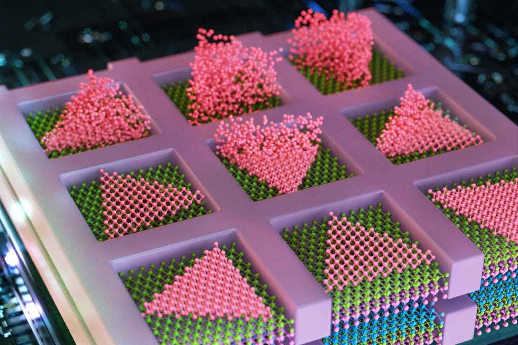
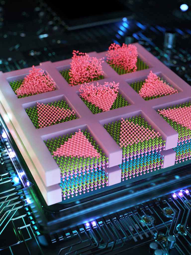
Researchers at École polytechnique fédérale de Lausanne (EPFL) have developed a technique to grow metals and ceramics within a water-based hydrogel. The team prints a hydrogel scaffold and infuses it with metal salts, then chemically transforms the salts into metallic nanoparticles. The researchers are able to realize geometrically intricate shapes called gyroids in various metals, such as copper and iron.
The gyroid lattices are formally complex, yet lightweight and strong. According to EPFL PhD student Yiming Ji, “Our materials could withstand 20 times more pressure compared to those produced with previous methods, while exhibiting only 20% shrinkage versus 60-90%.”
This abiotic growth process reverses the conventional fabrication sequence: rather than first choosing a material and then printing it, a scaffold is printed, and material selection and development occur afterwards. The resulting prints consist of high metal concentrations with minimal voids, and the reusable scaffold is resource-efficient.
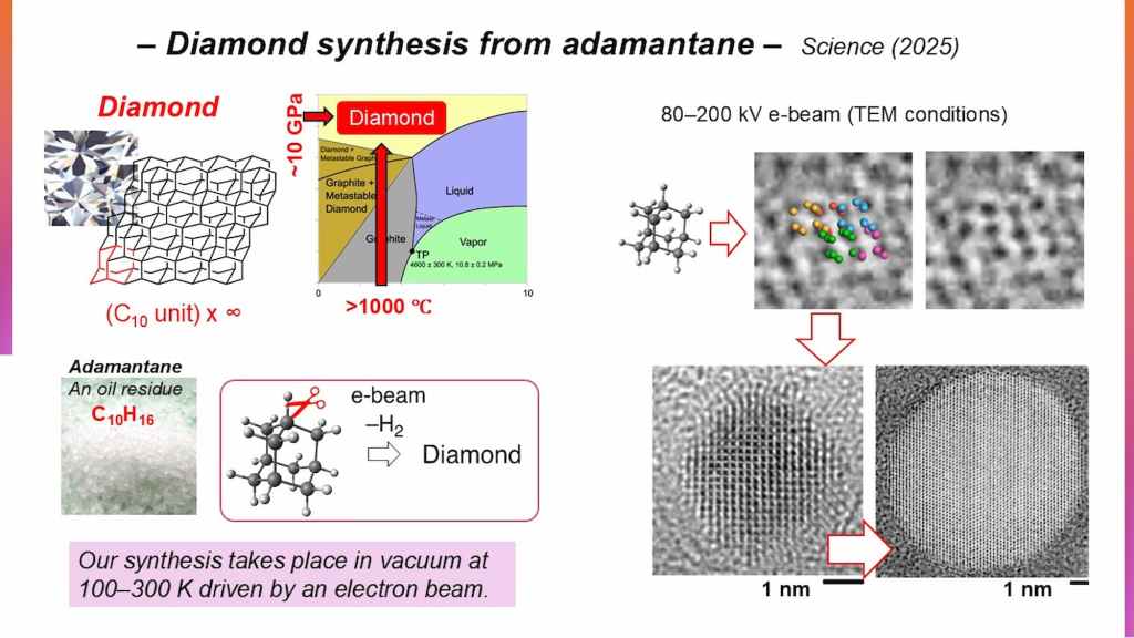
Another advancement enables the synthesis of diamond via an electron beam. Researchers at the University of Tokyo have demonstrated the capacity to grow nanodiamonds by exposing adamantane molecules to controlled electron irradiation. The process, which involves breaking C-H bonds to allow the formation of C-C bonds, results in cubic crystalline nanodiamonds up to 10 nm in diameter that are free of defects. What is notable about this contribution is the capability to create synthetic diamonds at relatively low heat and pressure—a significant improvement over the typical, extreme heat and pressure conditions required.
The researchers anticipate more distributed, site-based processing capability, such as growing diamonds from minerals found on meteorites via irradiation. The technology also holds promise for growing quantum dots for advanced sensors and computers. For architects and allied professionals, the diamond-growing process could lead to new coatings for surfaces, sensors, lenses, and other building products that offer unprecedented functional performance with a significantly lower environmental footprint, based on the greatly reduced processing energy required.
As the Internet of Things (IoT) is increasing the distribution and capacity of computational processing within the built environment, computer technology is taking inspiration from buildings. An MIT engineering team has devised a method to stack electrons in computer chips, taking advantage of the principle of vertical density found in skyscrapers. Similar to the contextual pressures and opportunities that motivate high-rise buildings, which greatly multiply the occupancy potential of a parcel of land, the MIT contribution dramatically increases the number of transistors and semiconductor devices that can occupy a particular area on a motherboard. The team achieves this feat by growing multilayered chips from semiconducting particles called transition-metal dichalcogenides (TMDs). The intricate stacking of these high-quality particles allows for volumetric density with streamlined communication, and requires less embodied energy via a process known as nucleating the edges.
Taking cues from architecture, the multilayer growth method offers something in return. As additive manufacturing develops in size, speed, and capacity, construction sites will increasingly feature onsite 3D printed building components. The MIT high-rise 3D chip approach demonstrates the potential for increased time and cost savings via incremental vertical growth (as opposed to more holistic methods requiring tower cranes)—a trend reinforced by techniques like high-speed slip-forming construction.
Collectively, these inventions demonstrate how the phenomenon of growth—presumed the exclusive domain of biology—may be realized in abiotic materials. Growing substances like metals and ceramics enables new possibilities for resource efficacy, structural integrity, communication, and other functional capacities.
Although these emerging contributions are limited in scale and not yet commercialized, they show literal and symbolic promise for the future built environment. In this future, buildings are increasingly grown versus assembled, and form and function are co-created by material processes rather than traditional design and construction methods. Such a vision invites architects and allied practitioners to contemplate how the logic of growth, rather than fabrication, will redefine future workflows, supply chains, and value propositions in architecture.